


Solid state drives (SSDs) are different from older, mechanical hard drives (HDDs) in many ways. The most obvious difference is that SSDs perform far better than HDDs in some respects - with far faster random access, particularly with many small files, for example. NVMe SSDs can also provide far higher maximum throughput. This comes at a cost: smaller capacities with a higher price per bit. But why are SSDs faster in this way? It’s because they rely on parallelization, derived from the way the flash is organized.
If you look at a SSD you will see one or more NAND packages/modules. M.2 drives tend to have these in an even amount - two, four, or eight packages - while 2.5” SSDs may have an uneven amount and, in times past, more than eight “chips.” These chips are actually one or more dies of flash that are stacked and wired together. The SSD’s controller can switch between these dies, that is to interleave, in order to improve performance. The ability to stack dies allows for better space usage with stacks typically going up to 8 or even 16 dies.

Die stacking. Source.
Each die has its own internal level of parallelization with two or more planes, with four becoming more common today. Each plane has its own circuitry so it can operate independently, and these planes can even operate on a sub-plane level in certain architectures. Each plane is made up of numerous blocks - the basic unit of erasure and garbage collection, or maintenance, for NAND SSDs. Each block is made up of many pages which tend to be 16KB in size for user data, with extra space set aside for functions such as error correction and for metadata.
Pages are known to be the smallest unit that can be written or read by the SSD, however given their size the ability to read a subpage - 4KB, which is typical for file systems - is a requirement. The page is made up of one cell for every bit but a given cell can handle more than one bit at a time, for example 3 bits with TLC. This means a TLC word line actually consists of three pages. The programming of these pages gets more difficult, and therefore slower, because increased sensitivity is required to differentiate the higher bit values. Since the value is determined by the cell's charge level, the cell is the atomic unit of NAND flash.

From cell to die package
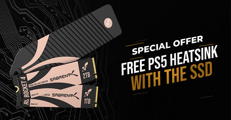
Our SSDs range all the way up to 8TB of TLC with the Rocket 4 Plus, requiring 8 NAND packages with 8 dies a piece. Our 4TB Rocket 4 Plus has the same amount of dies, but they are less dense. Those latter dies are four-plane, allowing for extra parallelization that offers unprecedented performance. All of this flash fits into a tiny M.2 2280 form factor, along with the controller and ample DRAM, a technological achievement for storage. Just consider how many cells there are in that drive, considering each cell only contains 3 bits!
See our storage products here.